I.C.E SYSTEM

Accelerated life testing for MEMS switch contacts

image091
In-Situ Contact Evolution (I.C.E) for MEMS ISO/ MIL Standard Compliant Contact Testing
High Speed Contact Switching (350 Million Operations/Day)
Ultra Precision Laser 3D Surface Mapping
Live Feedback from Colour Video Microscopy

Testing MEMS (Micro Electro Mechanical) switch contacts is a challenging problem as the MEMS switch operates at very low contact closure forces and must demonstrate hundreds of millions or billions of cycles to be practical. The sheer number of cycles means the testing time is extensive and often very little information is provided as to why the ultimate failure occurs.
TaiCaan have developed the In-Situ Evolution (ICE) system to investigate MEMS contact wear at nanometer scale during testing at high cyclic rates (4 kHz) – a capability previously unavailable to the MEMS contact developer. The system allows the contact lifetime to be established quickly and accurately extrapolated from a much lower number of cycles – speeding up testing and providing much greater diagnostic information.
This is achieved while the switching conditions (current, voltage, contact force and ambient environment) are closely controlled to simulate practical switching conditions.

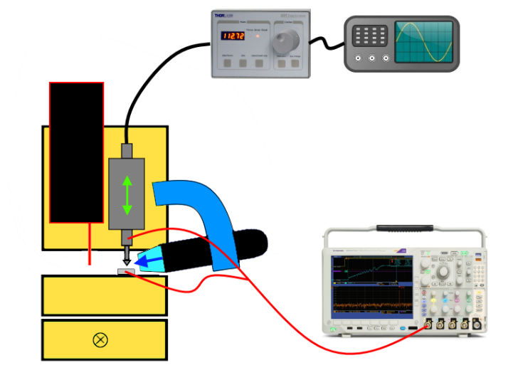
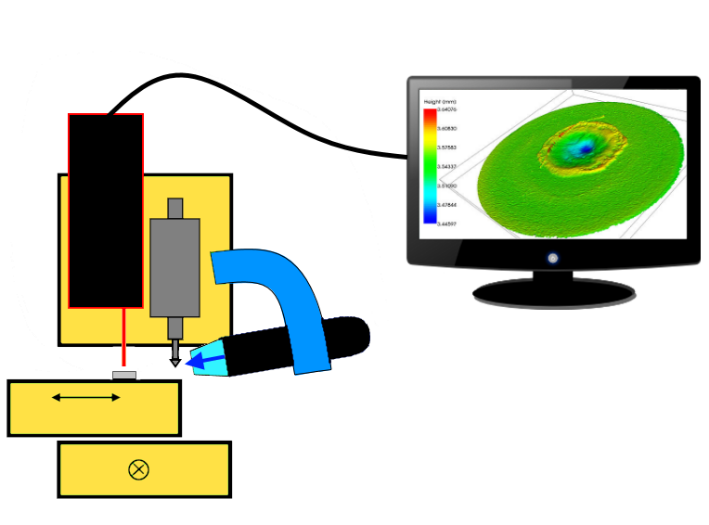
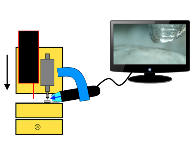
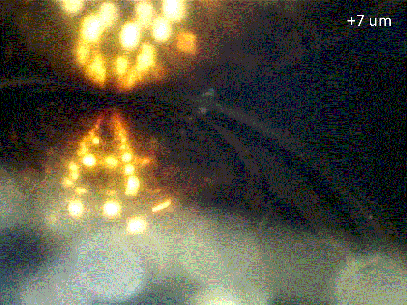
The sequence of images show the live operator view from the ICE Systems video microscope as a MEMS contact pair is operated for a single switching cycle.

The upper hemispherical contact is lowered towards a thin film planar contact. The contact surfaces have a highly reflective surface which reflects the image of the upper contact and the microscope light source.

The field of view is 250 x 150 um. The separation distance between the contacts is shown in micrometers (microns) as the number in the top right of the image.

MEMS Contact
MEMS Contact 2

A MEMS contact measured in-situ at the I.C.E System.

A 30 um wide patch of the 500 nm conductive film material delminates and transfers to the opposite contact after a single switching cycle. This can be seen as the lighter coloured region at the center of the image above.  The colour scale indicates height of the surface. Measurement region is 100 um wide and the film is 500 nm thick

The same region of the contact after a further 10 switching cycles. The colour scale and measurement region are the same as the previous image

Note: the upper right corner of the transfer patch has been transferred back to the opposing contact. The transfered film is also flatter than previous from more switching cycles.

Instrumentation indicates the contact is performing well at this stage. The contact fails catastrophically after many switching cycles by total delamination of the conductive film.

  • ISO/ MIL Standard Compliant (EN116000-3, MIL-R-83536/A, MIL-PRF-6106K, MIL-R-39016E)

  • Contact Force Measurement – Micro Newton (μN) Resolution

  • In Situ Surface Measurement (10 nm Height Resolution)

  • Measure Contact Between Switching Events

  • Full Instrument Data Logging

  • Programmable Operation

  • Simple User Interface

  • One Solution